- 您现在的位置:买卖IC网 > Sheet目录2003 > LTC1410IG#TR (Linear Technology)IC ADC 12BIT 1.25MSPS SMP 28SSOP
2
LTC1410
AVDD = DVDD = VDD (Notes 1, 2)
Supply Voltage (VDD) ................................................ 6V
Negative Supply Voltage (VSS) ............................... –6V
Total Supply Voltage (VDD to VSS) .......................... 12V
Analog Input Voltage
(Note 3) .................................. VSS – 0.3V to VDD + 0.3V
Digital Input Voltage (Note 4) ............ VSS – 0.3V to 10V
Digital Output Voltage ................... – 0.3V to VDD + 0.3V
Power Dissipation ............................................. 500mW
Operating Temperature Range
LTC1410C .............................................. 0
°C to 70°C
LTC1410I ........................................... – 40
°C to 85°C
Storage Temperature Range ................ – 65
°C to 150°C
Lead Temperature (Soldering, 10 sec)................. 300
°C
A
U
G
W
A
W
U
W
A
R
BSOLUTEXI
TI
S
WU
U
PACKAGE/ORDER I FOR ATIO
ORDER
PART NUMBER
Consult factory for Military grade parts.
PUT
U
I
A
U
LOG
PARAMETER
CONDITIONS
MIN
TYP
MAX
UNITS
Resolution (No Missing Codes)
q
12
Bits
Integral Linearity Error
(Note 7)
q
±0.3
±1
LSB
Differential Linearity Error
q
±0.3
±1
LSB
Offset Error
(Note 8)
±2
±6
LSB
q
±8
LSB
Full-Scale Error
±15
LSB
Full-Scale Tempco
IOUT(REF) = 0
q
±15
ppm/
°C
TJMAX = 110°C, θJA = 90°C/W (SW)
TJMAX = 110°C, θJA = 95°C/W (G)
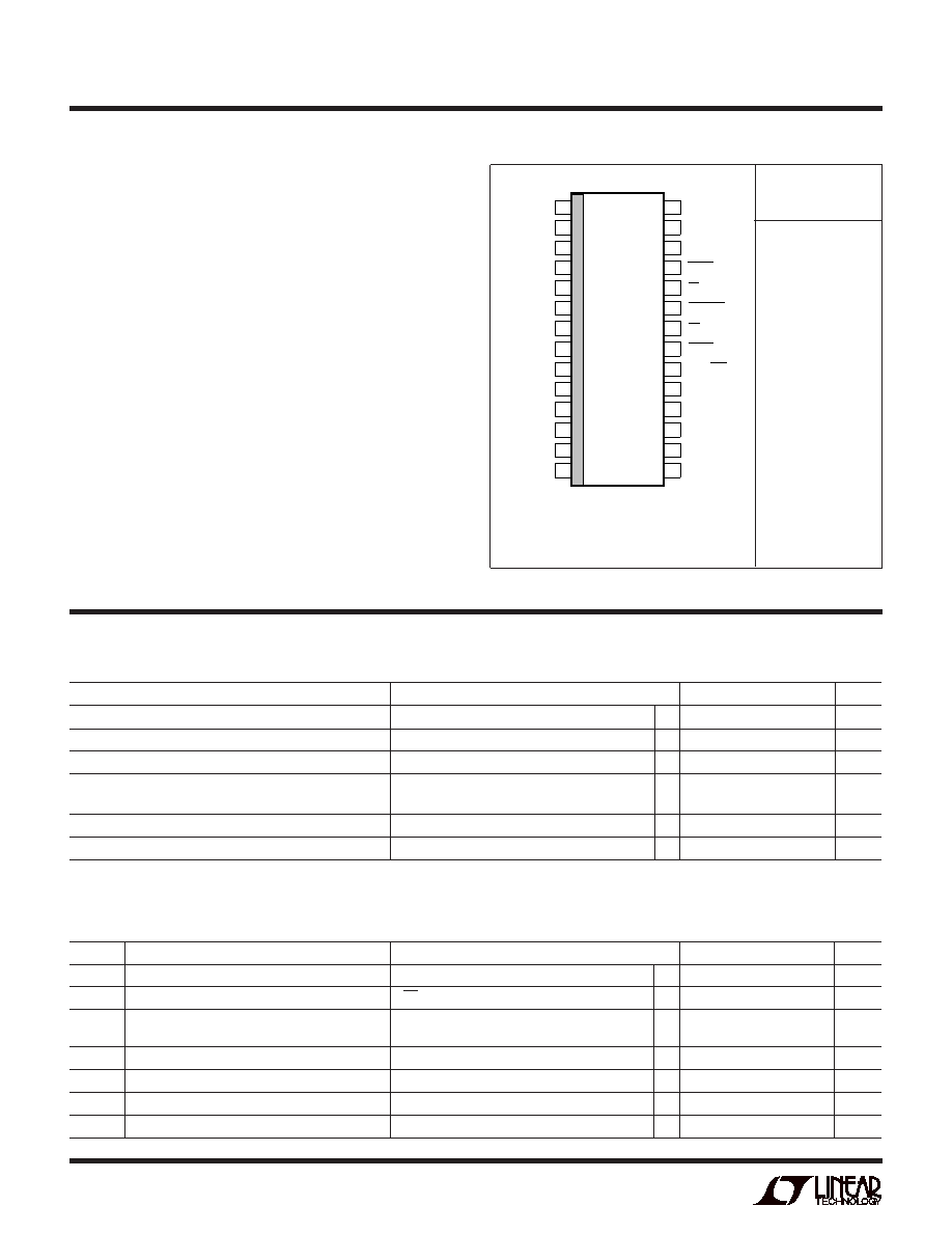
1
2
3
4
5
6
7
8
9
10
11
12
13
14
28
27
26
25
24
23
22
21
20
19
18
17
16
15
+AIN
–AIN
VREF
REFCOMP
AGND
D11(MSB)
D10
D9
D8
D7
D6
D5
D4
DGND
AVDD
DVDD
VSS
BUSY
CS
CONVST
RD
SHDN
NAP/SLP
OGND
D0
D1
D2
D3
G PACKAGE
28-LEAD PLASTIC SSOP
SW PACKAGE
28-LEAD PLASTIC SO WIDE
TOP VIEW
LTC1410CG
LTC1410CSW
LTC1410IG
LTC1410ISW
CC
HARA TERISTICS
CO
U
VERTER
The q denotes specifications which apply over the full operating
temperature range, otherwise specifications are at TA = 25°C. With Internal Reference (Notes 5, 6)
The q denotes specifications which apply over the full operating temperature range, otherwise
specifications are at TA = 25°C. (Note 5)
SYMBOL
PARAMETER
CONDITIONS
MIN
TYP
MAX
UNITS
VIN
Analog Input Range (Note 9)
4.75V
≤ VDD ≤ 5.25V, –5.25V ≤ VSS ≤ –4.75V q
±2.5
V
IIN
Analog Input Leakage Current
CS = High
q
±1
A
CIN
Analog Input Capacitance
Between Conversions
17
pF
During Conversions
5
pF
t ACQ
Sample-and-Hold Acquisition Time
q
50
100
ns
t AP
Sample-and-Hold Aperture Delay Time
–1.5
ns
tjitter
Sample-and-Hold Aperture Delay Time Jitter
5
psRMS
CMRR
Analog Input Common Mode Rejection Ratio
– 2.5V < (– AIN = AIN) < 2.5V
60
dB
发布紧急采购,3分钟左右您将得到回复。
相关PDF资料
LTC1411IG#TRPBF
IC A/D CONV 14BIT 2.5MSPS 36SSOP
LTC1412IG#TR
IC ADC 12BIT 3MSPS SAMPLE 28SSOP
LTC1414IGN#TRPBF
IC A/D CONV 14BIT SAMPLNG 28SSOP
LTC1415CG#TRPBF
IC A/D CONV 12BIT SAMPLNG 28SSOP
LTC1416IG#TR
IC ADC 14BIT 400KSPS SMPL 28SSOP
LTC1417AIGN#TR
IC ADC 14BIT 400KSPS SMPL 16SSOP
LTC1418ACG#TRPBF
IC A/D CONV 14BIT SRL&PAR 28SSOP
LTC1419AISW#TRPBF
IC A/D CONV 14BIT SAMPLNG 28SOIC
相关代理商/技术参数
LTC1410IG#TRPBF
功能描述:IC A/D CONV 12BIT SAMPLNG 28SSOP RoHS:是 类别:集成电路 (IC) >> 数据采集 - 模数转换器 系列:- 标准包装:1,000 系列:- 位数:12 采样率(每秒):300k 数据接口:并联 转换器数目:1 功率耗散(最大):75mW 电压电源:单电源 工作温度:0°C ~ 70°C 安装类型:表面贴装 封装/外壳:24-SOIC(0.295",7.50mm 宽) 供应商设备封装:24-SOIC 包装:带卷 (TR) 输入数目和类型:1 个单端,单极;1 个单端,双极
LTC1410ISW
功能描述:IC A/D CONV 12BIT SAMPLNG 28SOIC RoHS:否 类别:集成电路 (IC) >> 数据采集 - 模数转换器 系列:- 标准包装:1,000 系列:- 位数:12 采样率(每秒):300k 数据接口:并联 转换器数目:1 功率耗散(最大):75mW 电压电源:单电源 工作温度:0°C ~ 70°C 安装类型:表面贴装 封装/外壳:24-SOIC(0.295",7.50mm 宽) 供应商设备封装:24-SOIC 包装:带卷 (TR) 输入数目和类型:1 个单端,单极;1 个单端,双极
LTC1410ISW#PBF
功能描述:IC A/D CONV 12BIT SAMPLNG 28SOIC RoHS:是 类别:集成电路 (IC) >> 数据采集 - 模数转换器 系列:- 标准包装:1,000 系列:- 位数:12 采样率(每秒):300k 数据接口:并联 转换器数目:1 功率耗散(最大):75mW 电压电源:单电源 工作温度:0°C ~ 70°C 安装类型:表面贴装 封装/外壳:24-SOIC(0.295",7.50mm 宽) 供应商设备封装:24-SOIC 包装:带卷 (TR) 输入数目和类型:1 个单端,单极;1 个单端,双极
LTC1410ISW#TR
功能描述:IC ADC 12BIT 1.25MSPS SMP 28SOIC RoHS:否 类别:集成电路 (IC) >> 数据采集 - 模数转换器 系列:- 标准包装:1,000 系列:- 位数:12 采样率(每秒):300k 数据接口:并联 转换器数目:1 功率耗散(最大):75mW 电压电源:单电源 工作温度:0°C ~ 70°C 安装类型:表面贴装 封装/外壳:24-SOIC(0.295",7.50mm 宽) 供应商设备封装:24-SOIC 包装:带卷 (TR) 输入数目和类型:1 个单端,单极;1 个单端,双极
LTC1410ISW#TRPBF
功能描述:IC A/D CONV 12BIT SAMPLNG 28SOIC RoHS:是 类别:集成电路 (IC) >> 数据采集 - 模数转换器 系列:- 标准包装:1,000 系列:- 位数:12 采样率(每秒):300k 数据接口:并联 转换器数目:1 功率耗散(最大):75mW 电压电源:单电源 工作温度:0°C ~ 70°C 安装类型:表面贴装 封装/外壳:24-SOIC(0.295",7.50mm 宽) 供应商设备封装:24-SOIC 包装:带卷 (TR) 输入数目和类型:1 个单端,单极;1 个单端,双极
LTC1411CG
功能描述:IC A/D CONV 14BIT 2.5MSPS 36SSOP RoHS:否 类别:集成电路 (IC) >> 数据采集 - 模数转换器 系列:- 标准包装:1 系列:- 位数:14 采样率(每秒):83k 数据接口:串行,并联 转换器数目:1 功率耗散(最大):95mW 电压电源:双 ± 工作温度:0°C ~ 70°C 安装类型:通孔 封装/外壳:28-DIP(0.600",15.24mm) 供应商设备封装:28-PDIP 包装:管件 输入数目和类型:1 个单端,双极
LTC1411CG#PBF
功能描述:IC ADC 14BIT 2.5MSPS 36SSOP RoHS:是 类别:集成电路 (IC) >> 数据采集 - 模数转换器 系列:- 标准包装:1 系列:- 位数:14 采样率(每秒):83k 数据接口:串行,并联 转换器数目:1 功率耗散(最大):95mW 电压电源:双 ± 工作温度:0°C ~ 70°C 安装类型:通孔 封装/外壳:28-DIP(0.600",15.24mm) 供应商设备封装:28-PDIP 包装:管件 输入数目和类型:1 个单端,双极
LTC1411CG#TR
功能描述:IC A/D CONV 14BIT 2.5MSPS 36SSOP RoHS:否 类别:集成电路 (IC) >> 数据采集 - 模数转换器 系列:- 标准包装:1 系列:- 位数:14 采样率(每秒):83k 数据接口:串行,并联 转换器数目:1 功率耗散(最大):95mW 电压电源:双 ± 工作温度:0°C ~ 70°C 安装类型:通孔 封装/外壳:28-DIP(0.600",15.24mm) 供应商设备封装:28-PDIP 包装:管件 输入数目和类型:1 个单端,双极